- 您现在的位置:买卖IC网 > Sheet目录1228 > MAX4273EVKIT (Maxim Integrated Products)EVAL KIT FOR MAX4273
�� �
�
�3V� to� 12V� Current-Limiting� Hot-Swap� Controllers�
�with� Autoretry,� DualSpeed/BiLevel� Fault� Protection�
�is� stable.� Any� input� voltage� transient� at� IN� below� the�
�UVLO� threshold� will� reset� the� device� and� initiate� a� start-�
�up� sequence.�
�These� devices� also� have� an� overvoltage� lockout�
�(OVLO)� feature� that� prevents� the� device� from� restarting�
�after� a� fault� condition� if� the� discharge� has� not� been�
�completed.� V� GATE� has� to� be� discharged� to� below� 0.1V.�
�Additionally,� the� MAX4273� LLMON� pin� discharges� the�
�load� line� with� a� 1k� Ω� pulldown� and� prevents� startup� until�
�the� load� voltage� is� below� 0.1V.�
�Since� the� MAX4271/MAX4272� do� not� monitor� the� output�
�voltage,� a� startup� sequence� can� be� initiated� while� the�
�board� capacitance� is� still� charged.�
�A� large� board� capacitance� or� a� short� startup� period� may�
�prevent� the� MAX4272� from� charging� completely� in� one�
�startup� period.� The� MAX4272� responds� to� these� condi-�
�tions� by� charging� the� capacitor� with� bursts� defined� by� a�
�t� ON� duty� cycle� and� a� period� of� t� ON� +� t� RETRY� .� The� charg-�
�ing� will� be� complete� after� several� retries� unless� the� resis-�
�Applications� Information�
�Component� Selection�
�N-Channel� MOSFET�
�Select� the� external� N-channel� MOSFET� according� to�
�the� application’s� current� level.� Table� 2� lists� some� rec-�
�ommended� components.� The� MOSFET’s� on-resistance�
�(R� DS(ON)� )� should� be� chosen� low� enough� to� have� a� min-�
�imum� voltage� drop� at� full� load� to� limit� the� MOSFET�
�power� dissipation.� High� R� DS(ON)� can� cause� output� rip-�
�ple� if� the� board� has� pulsing� loads� or� triggers� an� exter-�
�nal� undervoltage� reset� monitor� at� full� load.� Determine�
�the� device� power-rating� requirement� to� accommodate�
�a� short� circuit� on� the� board� at� startup� with� the� device�
�IN�
�R� SENSE�
�tive� load� or� current� load� excessively� discharges� the�
�board� capacitance� during� the� retry� timeout.� This� feature�
�applies� to� the� MAX4273� if� LLMON� is� left� floating� or� is�
�connected� to� GND.� To� prevent� multiple� charging� bursts,�
�ensure� that� the� t� ON� timer� exceeds� the� minimum� time�
�MAX4271�
�MAX4272�
�SENSE�
�V� GD�
�required� to� complete� the� charge� of� the� board� capaci-�
�tance� (see� Component� Selection� ).�
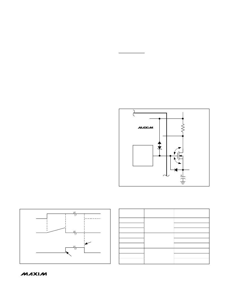
�Gate� Overvoltage� Protection�
�New-generation� MOSFETs� have� an� absolute� maximum�
�rating� of� ±8V� for� the� gate-to-source� voltage� (V� GS� ).� To�
�GATE� DRIVE�
�CHARGE� PUMP�
�GATE�
�V� GS�
�D1�
�M1�
�N�
�V� OUT�
�protect� these� MOSFETs,� the� MAX4271/MAX4272� limit� the�
�gate-to-drain� voltage� (the� MAX4273� limits� the� gate-to-�
�source� voltage)� to� +7.5V� with� an� internal� zener� diode.� No�
�protection� is� provided� for� negative� V� GS� (MAX4271/�
�MAX4272).� If� GATE� can� be� discharged� to� ground� faster�
�than� the� output� voltage,� an� external� small-signal� protec-�
�tion� diode� (D1)� can� be� used,� as� shown� in� Figure� 6.� The�
�MAX4273� has� the� protection� diode� internal.�
�C� BOARD�
�Figure� 6.� External� Gate-Source� Protection�
�Table� 2.� Recommended� N-Channel�
�MOSFETs�
�ON�
�CTIM�
�(CTON)*�
�STAT�
�V� IN�
�O�
�1.2V�
�O�
�V� IN�
�O�
�t� START�
�FAULT� CONDITION,�
�OR� ON� FALLING�
�EDGE�
�NO� FAULT� CONDITIONS� PRESENT�
�PART�
�NUMBER�
�IRF7413�
�IRF7401�
�IRL3502S�
�MMSF3300�
�MMSF5N02H�
�MTB60N05H�
�FDS6670A�
�NDS8426A�
�MANUFACTURER�
�International�
�Rectifier�
�Motorola�
�Fairchild�
�DESCRIPTION�
�11m� Ω� ,� 8� SO,� 30V�
�22m� Ω� ,� 8� SO,� 20V�
�6m� Ω� ,� D2PAK,� 20V�
�20m� Ω� ,� 8� SO,� 30V�
�30m� Ω� ,� 8� SO,� 20V�
�14m� Ω� ,� D2PAK,� 50V�
�10m� Ω� ,� 8� SO,� 30V�
�13.5m� Ω� ,� 8� SO,� 20V�
�*MAX4273� ONLY�
�Figure� 5.� Status� (STAT)� Output� Timing� Diagram�
�FDB8030L�
�4.5m� Ω� ,� D2PAK,� 30V�
�______________________________________________________________________________________�
�15�
�发布紧急采购,3分钟左右您将得到回复。
相关PDF资料
MAX4278EVKIT-SO
KIT EVALUATION FOR MAX4178,4278
MAX44265EVKIT#
KIT EVAL FOR 44265
MAX4754AEVKIT+
KIT EVAL FOR MAX4754
MAX4810EVKIT+
KIT EVAL FOR MAX4810
MAX4886EVKIT+
KIT EVAL FOR MAX4886
MAX4948EVKIT+
KIT EVAL FOR MAX4948
MAX4983EEVKIT+
KIT EVAL FOR MAX4983
MAX4989EVKIT+
EVALUATION KIT FOR MAX4989
相关代理商/技术参数
MAX4274ABESA
功能描述:运算放大器 - 运放 Integrated Circuits (ICs)
RoHS:否 制造商:STMicroelectronics 通道数量:4 共模抑制比(最小值):63 dB 输入补偿电压:1 mV 输入偏流(最大值):10 pA 工作电源电压:2.7 V to 5.5 V 安装风格:SMD/SMT 封装 / 箱体:QFN-16 转换速度:0.89 V/us 关闭:No 输出电流:55 mA 最大工作温度:+ 125 C 封装:Reel
MAX4274ABESA+T
功能描述:运算放大器 - 运放 RoHS:否 制造商:STMicroelectronics 通道数量:4 共模抑制比(最小值):63 dB 输入补偿电压:1 mV 输入偏流(最大值):10 pA 工作电源电压:2.7 V to 5.5 V 安装风格:SMD/SMT 封装 / 箱体:QFN-16 转换速度:0.89 V/us 关闭:No 输出电流:55 mA 最大工作温度:+ 125 C 封装:Reel
MAX4274ABESA-T
功能描述:运算放大器 - 运放
RoHS:否 制造商:STMicroelectronics 通道数量:4 共模抑制比(最小值):63 dB 输入补偿电压:1 mV 输入偏流(最大值):10 pA 工作电源电压:2.7 V to 5.5 V 安装风格:SMD/SMT 封装 / 箱体:QFN-16 转换速度:0.89 V/us 关闭:No 输出电流:55 mA 最大工作温度:+ 125 C 封装:Reel
MAX4274ABEUA
功能描述:运算放大器 - 运放 Integrated Circuits (ICs)
RoHS:否 制造商:STMicroelectronics 通道数量:4 共模抑制比(最小值):63 dB 输入补偿电压:1 mV 输入偏流(最大值):10 pA 工作电源电压:2.7 V to 5.5 V 安装风格:SMD/SMT 封装 / 箱体:QFN-16 转换速度:0.89 V/us 关闭:No 输出电流:55 mA 最大工作温度:+ 125 C 封装:Reel
MAX4274ABEUA-T
功能描述:运算放大器 - 运放
RoHS:否 制造商:STMicroelectronics 通道数量:4 共模抑制比(最小值):63 dB 输入补偿电压:1 mV 输入偏流(最大值):10 pA 工作电源电压:2.7 V to 5.5 V 安装风格:SMD/SMT 封装 / 箱体:QFN-16 转换速度:0.89 V/us 关闭:No 输出电流:55 mA 最大工作温度:+ 125 C 封装:Reel
MAX4274ACESA
功能描述:运算放大器 - 运放
RoHS:否 制造商:STMicroelectronics 通道数量:4 共模抑制比(最小值):63 dB 输入补偿电压:1 mV 输入偏流(最大值):10 pA 工作电源电压:2.7 V to 5.5 V 安装风格:SMD/SMT 封装 / 箱体:QFN-16 转换速度:0.89 V/us 关闭:No 输出电流:55 mA 最大工作温度:+ 125 C 封装:Reel
MAX4274ACESA-T
功能描述:运算放大器 - 运放
RoHS:否 制造商:STMicroelectronics 通道数量:4 共模抑制比(最小值):63 dB 输入补偿电压:1 mV 输入偏流(最大值):10 pA 工作电源电压:2.7 V to 5.5 V 安装风格:SMD/SMT 封装 / 箱体:QFN-16 转换速度:0.89 V/us 关闭:No 输出电流:55 mA 最大工作温度:+ 125 C 封装:Reel
MAX4274ACEUA
功能描述:运算放大器 - 运放
RoHS:否 制造商:STMicroelectronics 通道数量:4 共模抑制比(最小值):63 dB 输入补偿电压:1 mV 输入偏流(最大值):10 pA 工作电源电压:2.7 V to 5.5 V 安装风格:SMD/SMT 封装 / 箱体:QFN-16 转换速度:0.89 V/us 关闭:No 输出电流:55 mA 最大工作温度:+ 125 C 封装:Reel